Prasad Soman will graduate soon with his PhD in Materials Science and Engineering. But instead of walking down the aisle and tossing his cap in Michigan Tech’s Dee Stadium, this year he’ll take part in Michigan Tech’s first-ever outdoor graduation walk.
“My PhD research goal was to better understand how the addition of carbon affects the strengthening mechanism of iron—by looking to see what happens at the nanoscale,” he explains.
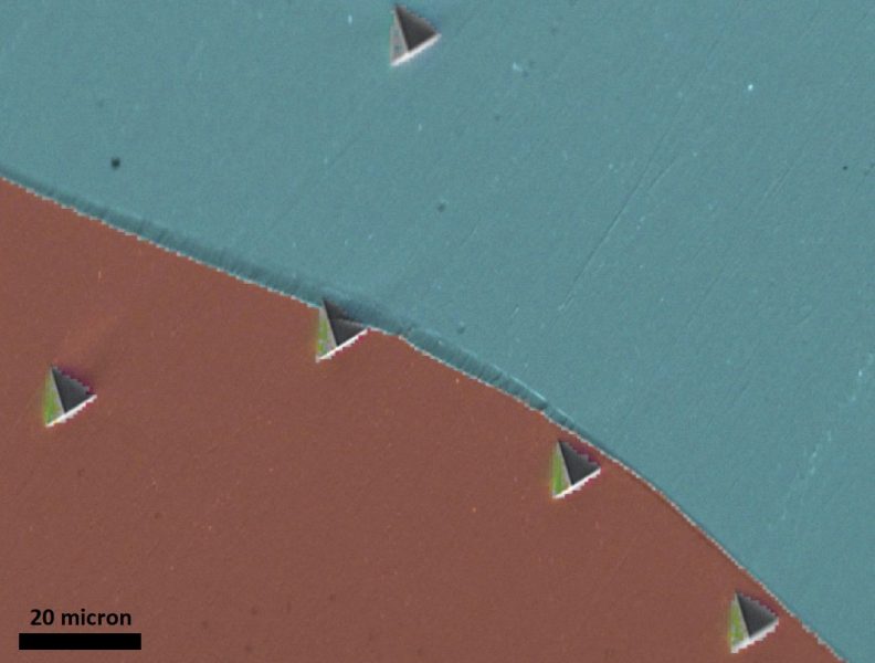
Soman studied the mechanisms of grain boundary strengthening by using an advanced and challenging technique known as nanoindentation to get “up close and personal” to the interfaces between individual crystals within a material. Just last week Soman successfully defended his PhD dissertation: “Study of Effects of Chemistry and Grain Boundary Geometry on Materials Failure.” The research was sponsored by the US Department of Energy.
He’ll soon be moving to California to take a position with Amazon, the culmination of many years of hard work. “My journey into the field of metallurgy and materials science began in India, way back in high school, when I was thinking of choosing a major for my undergraduate studies in engineering. I had developed a great interest in Physics and Chemistry, then discovered I could pursue my interest even further by choosing metallurgical engineering as my major,” he says.
Though his new position will not utilize his metallurgical expertise in a direct way, Amazon was drawn to Prasad’s ability to independently carry out and complete a detailed research project that required a high level of attention to detail, data collection, and advanced analysis and physical modeling.
“I attended College of Engineering Pune, one of the top tier schools for metallurgy in India. Upon graduation, I went on to work in the steel industry for a while, and then decided to pursue higher education in the US.
Soman arrived at Michigan Tech with the intention of earning a Master’s in MSE. Professor Yun Hang Hu advised Soman towards that degree, involving him in research focused on the fabrication and characterization of Molybdenum Disulfide (MoS2)-based electrodes (aka Moly) for supercapacitor applications. The experience prompted Soman to continue on in his studies and earn a PhD.
Two MSE faculty members, Assistant Professor Erik Herbert and Professor Stephen Hackney, served as Soman’s PhD co-advisors. “Prasad analyzed the effect of grain boundary segregation on the strengthening and deformation mechanism in metals and alloys,” says Herbert. “To do this Prasad intensively used small-scale mechanical testing, including nanoindentation and in-situ TEM experiments.”
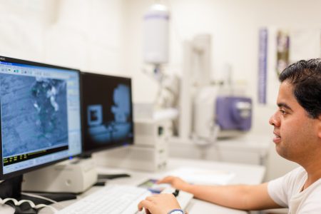
“The most exciting part of this work involved utilizing various material characterization techniques,” says Soman. “The Advanced Chemical and Morphological Analysis Laboratory (ACMAL) facility, located in the Michigan Tech M&M building near the MSE department, is one of the best materials characterization facilities in the world. Characterization of the materials response to mechanical indentation was essential for my PhD work, so having access to the many techniques available in ACMAL was both revealing and fulfilling.”
“The work was painstaking, but thanks to Prasad’s incredible hard work, skill, and dedication, he was able to make significant inroads to improve our understanding.”
Soman used a variety of characterization methods in his research, including nanoindentation, scanning electron microscopy (SEM), transmission electron microscopy (TEM), and electron backscatter diffraction spectroscopy (EBSD). “All help examine materials behavior at the nanometer scale,” he adds.

In particular, Soman used nanoindentation to study local grain boundary deformation in metals and alloys. “Using nanoindentation we can measure hardness at a very small length scale. The indentation impression size is on the order of a couple of microns—smaller than the width of a human hair,” Soman explains.
“Performing a nanoindentation was challenging at first. The goal is to get the indentation very close to the grain boundary. The task is done using a simple optical microscope, yet accuracy on the order of a couple of microns must be achieved. That kind of accuracy is essential for the proper positioning of the indent relative to the boundary. But just as for any other thing, the more you practice (and learn from mistakes) the better you perform. It’s been a great achievement for me to consistently get the indentation accurately placed.”
“Instrumented indentation experiments allow us to measure materials properties—including hardness and elastic modulus—as a function of depth,” says Soman. “We also examine how different microstructural features—grain boundary vs. grain interior—respond to a very localized deformation at nanometers length scale.”
Soman says he decided to join Michigan Tech’s MSE program due to its strong emphasis on metallurgical engineering. “While here at Tech, however, I was exposed to a variety of domains within materials science—energy storage materials, semiconductors, polymers, and more. So, while I focused on my passion for fundamental science in metallurgy, I also developed understanding and skills in these different domains,” he explains.
“That has come to fruition, as I will now be going to work in the consumer electronics industry, which requires a multidisciplinary approach.”

Soman will soon pack up and move to Sunnyvale, California. He’ll be working as a hardware development engineer at Amazon. “The team is a cool group of engineers/scientists with diverse backgrounds—mechanical, chemical, design and other disciplines, as well. We’ll develop health and wellness electronic devices, such as smart watches, smart AR/VR glasses, and more. This job will allow me to utilize some of the key skills I developed at Michigan Tech in the field of metallurgy and mechanics. More than anything, I am eager to learn from the best of the best—all the folks in my team.”
One last thing, adds Soman: “I will terribly miss Houghton. I call it my home away from home.”