Category: News

ACMAL Works with Students on SEM Video Solution

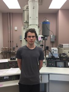
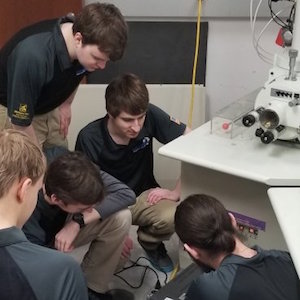
Students by the SEMBlue Marble Security, born out of the Michigan Tech Enterprise program, is a virtual company comprised of American and international undergraduate students focused on securing the future through thoughtful use of technology.

The project Paul Sanders proposed to Glen Archer was straightforward enough — make something old new again. Sanders came upon the challenge through a former colleague at Ford Motor Company, James Boileau.

The company’s goal was to replace the CRT monitors with off-the-shelf LED displays, similar to what you would find in most office computers.

The students were given access to Tech’s JEOL 6400. In addition, Owen Mills, senior research engineer and director of the Applied Chemical and Morphological Analysis Laboratory in the Department of Materials Science and Engineering, provided printed schematics, operations and maintenance manuals. The search for a place to tap the video signals required the visual inspection and search of hundreds of pages of printed schematics. Finally Blue Marble found what they were looking for — a low-voltage signal in an early video display protocol pioneered by IBM called monochrome display adapter (MDA).

Read more at Michigan Tech News, by Mark Wilcox.

Award Winning Adhesives Researcher Credits ACMAL Expertise

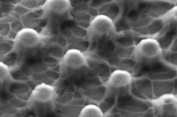
Micrograph of micropillar array
Adhesive-coated pillars made using a a silicon template provided by Microfabrication Facility Managing Director Chito Kendrick. The morphology was visualized using the ACMAL E-SEM with the help of Lab Supervisor Jerry Anzalone.

The Bhakta Rath Research Award honors a graduate student and faculty mentor for in-depth work with social impact. The 2019 winners are two biomedical engineers with a sticky past.

A smart adhesive doesn’t adhere all the time. In 2015, when Ameya Narkar started his doctoral research with Bruce Lee, associate professor of biomedical engineering at Michigan Technological University, the two turned to biological sources for a glue that could be turned on and off.

Q: How have your methods helped make the project successful?

Ameya Narkar: Our biomedical engineering department is full of approachable experts. It’s a small team and an effective one. I could walk down to a faculty member’s office and ask for advice when our project branched into areas beyond our lab’s expertise. Plus, I was able to work closely with the people in the Applied Chemical and Morphological Analysis Laboratory and the microfabrication facility. Collaboration is essential to successful research.

Read more at Michigan Tech News, by Allison Mills.

Course in Surface and Interface Science

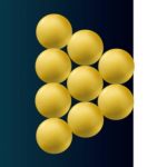
Surface ArraySurface and Interface Science CH5665/MSE5665
(3 credits)
WF 1-2 p.m., M 1-4 p.m. (lab)

Course Description – covers an advanced study of:

  • surface processes
  • properties of crystalline surfaces
  • surface analysis methods
  • applications towards materials science, heterogeneous catalysis, environmental science, semiconductor and energy industries

Objectives

  • Understand the physical and chemical processes on a surface
  • Distinguish differences between surface science techniques and their respective capabilities
  • Analyze example data from surface science techniques
  • Recognize, review and interpret surface science literature
  • Design an experiment (or project) and choose a surface science technique that would solve a proposed hypothesis

For more information contact:

Dr. Kathryn A. Perrine
kaperrin@mtu.edu

View the Flyer

Gold Quantum Dots Observed with S-TEM

Gold Quantum DotYoke Khin Yap, professor of physics at Michigan Tech, led the study. He explains that the behavior his team observed — atomic-level manipulation of gold quantum dots — can be seen with a scanning transmission electron microscope (STEM). The STEM’s high-powered beam of electrons enables researchers like Yap to watch atomic movement in real-time and the view reveals how gold atoms interact with the surface of boron nitride nanotubes. Basically, the gold atoms glide along the surface of the nanotubes and, they stabilize in a hover just above the hexagon honeycomb of the boron nitride nanotubes.

Read more at Michigan Tech News, by Allison Mills.

Related:

Atomic Zoom: Michigan Tech’s Scanning Transmission Electron Microscope

S-TEM Images for Al-Sc Alloy

S-TEM Al Sc imagesPaul Sanders, Patrick Horvath Endowed Associate Professor of materials science and engineering, and materials science and engineering graduate student Yang Yang, are trying to strengthen aluminum by adding scandium to it.

The aberration-corrected FEI Titan Themis scanning transmission electron microscope (STEM) in Michigan Tech’s Applied Chemical and Morphological Analysis Laboratory, makes an electron beam less than an atom in width. This allows researchers to scan through samples one atom column at a time. Additionally, the lab has a SuperXTM X-ray detector, which is an array of four detectors to collect four times more X-rays than a conventional detector.

Combining the two techniques, researchers can element map at atomic resolution.

Read more at Unscripted, by Kelley Christensen.

Related:

S-TEM Provides Insight to Alloy Behavior

New EOF Lab Assistant Elizabeth (Fraki) Miller

Elizabeth (Fraki) Miller

My name is Elizabeth (Fraki) Miller. I have a bachelor’s degree in Forest Science from Michigan Tech. I am highly involved with several local groups including Ski Tigers, Singletrack Flyers, the SöKē Trails, and the Keweenaw Homeschoolers. I am interested in Nutritional Biochemistry and plan to pursue a Master’s Degree in Chemistry. I enjoy mountain biking, weight lifting, yoga, and cross country skiing.

S-TEM Provides Insight to Alloy Behavior

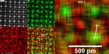
S-TEM MappingMaterials Science doctoral candidate Deji Fadayomi, and professors Paul Sanders and Gregory Odegard, are working on these precipitation-strengthening mechanisms in aluminum-based alloys. This atomic-resolution image and elemental maps of precipitates were obtained in aberration-corrected scanning transmission electron microscope (AC-STEM) at Michigan Tech’s Applied Chemical and Morphological Analysis Laboratory (ACMAL) to better understand alloy behavior at an atomic level.

Read more at Be Brief: Strength, by Kelley Christensen.

S-TEM Live Lab Tour Video Spring 2018

Michigan Tech faculty and staff presented a live tour of the FEI 200kV Titan Themis S-TEM facility on Facebook last Wednesday, February 14, 2018.

Introducing the tour was Kelley Christensen, science and technology publications writer for University Marketing and Communications. Steve Hackney, a professor in the Department of Materials Science and Engineering, talked about the atomic scale science and engineering taking place in the housing facility, the Advanced Technology Development Complex (ATDC).

ACMAL Director Owen Mills discussed sample preparation procedures. S-TEM specialist Pinaki Mukherjee demonstrated operation of the instrument and its capabilities.

Facebook Video | YouTube Video

Related:

Atomic Zoom: Michigan Tech’s Scanning Transmission Electron Microscope

Danielle Langdon

Danielle Langdon
Danielle Langdon

Danielle Langdon is a new lab assistant in the Electron Optics Facility, working under Owen Mills.

My name is Danielle Langdon. I am currently an undergraduate student in Michigan Tech’s Chemistry program. I’ve lived in the Copper Country for half of my life now and graduated from Hancock Central High. While I was in high school I was active JROTC and Drill Team. I am currently finishing my undergraduate degree and will be graduating in the Spring of 2017. After I graduate, I am interested in pursuing a career in Forensics. When I am not in school or working, I enjoy kayaking, rugby, and self-taught programming.