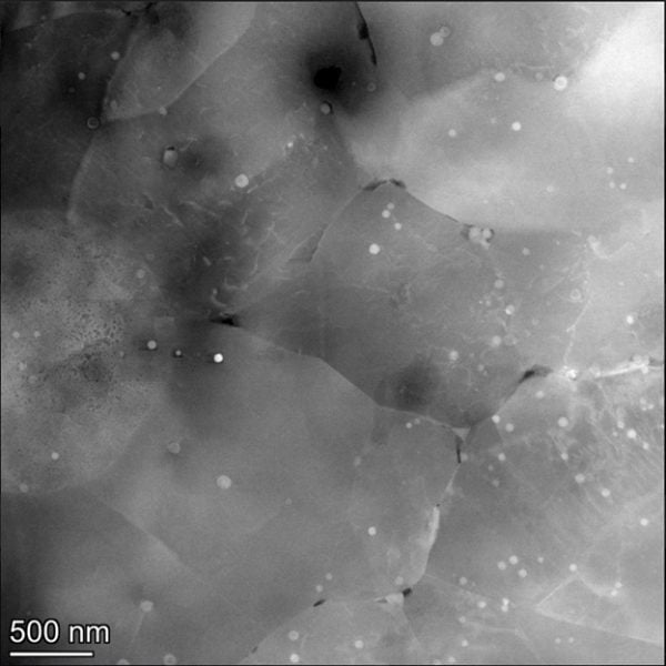
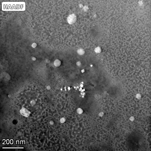
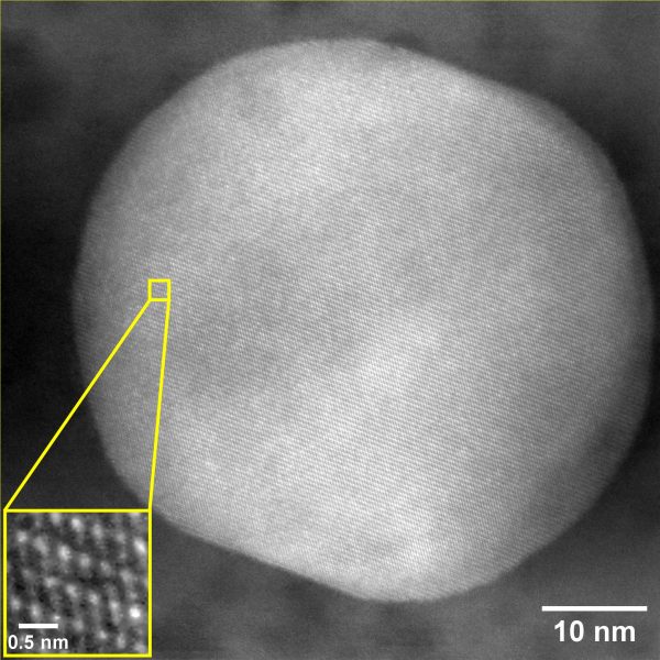
A materials science and engineering team of students Sonja Blickley, Tori Nizzi, Anna Palmcook, and Austin Schaub were sponsored by Hobart Brothers LLC. (Hobartbrothers.com) to develop a new process that has yielded some exciting results. Working with Dr. Erico Freitas, operator of the Titan Themis Scanning Electron Microscope, these students used the FEI 200kV Titan Themis Scanning Transmission Electron Microscope (STEM) to produce some awesome images of a welded material. They have granted special permission to show these pictures here, despite wishing to keep their work and the composition of their material confidential.
This team is very excited about their results, which help to drive the science of materials and engineering forward. Congratulations to them for their hard work paying off!
By Joshua Jongema.