The Fiber-lite on the AFM isn’t working properly. I believe it may be a blown fuse. Unfortunately, I’m unable to find a replacement locally. I have placed an order online which is scheduled to arrive on Monday.
I was able to replace the rod and the issue is resolved.
Please don’t ever force anything on the microscopes. If there is an issue you can call me. If I’m not available you can send me an email and I will take care of it as soon as I can.
The FESEM is down. The specimen exchange rod has been bent making it almost impossible to load a sample.
There is an issue with the stage of the TEM that is preventing it from changing X, Y, and Z coordinates.
The service engineer should be on site next Tuesday Jan. 17 to get that fixed.
I hope the TEM will be back by Thursday next week.
Regards,
Erico Freitas
One of the medium sized LN2 dewars has two missing fittings. If anyone knows where they may have gone to please let me know.
ACMAL will have limited hours over the upcoming holiday break.
During the week of December 19th-23rd, the labs will be open with limited staffing. The university, including ACMAL, will be closed on Dec 26th through 31st. The building will be locked on those days. Unrestricted users will still have access to the building and labs.
I will be out of the office but in the area, for the next two weeks. Josh King and Zoe Hoffman will be out as well. Dr. Erico Fritas will be available through Wednesday Dec 21st. Dr. Ed Laitila, Dr. Tim Leftwich, Aleister Kerr, Maci Dostaler will be available by appointment.
If there are problems contact us. Our contact information is:
Liz: 906-370-6538
Ed: 906-369-2041
Erico: 906-299-2714
Tim: trleftwi@mtu.edu
Happy Holidays,
Elizabeth Miller

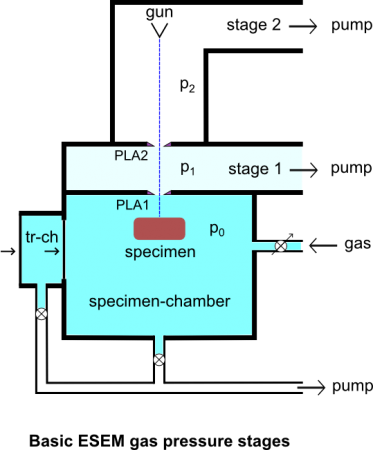
Basic ESEM gas pressure stages, by Gerry Danilatos.
The Department of Defense (DoD) announces the Fiscal Year 2023 Defense University Research Instrumentation Program (DURIP). I’m excited to share that the 2023 DURIP selections have been announced and our proposal for a new Environmental Scanning Electron Microscope is recommended for award. All indications are that it will be funded. Congratulations to Dr. Bruce Lee (PI), Dr. Paul Sanders, Dr. Trisha Sain, Dr. Kazuya Tajiri, and Dr. Stephen Techtmann. Once funded, the new instrument will be housed in ACMAL and available for use by the MTU research community.
The timing is still TBD but since the project should be completed within a year we are starting the planning process to finalize the equipment purchase. However, there is still an opportunity to add capabilities to the instrument, especially if cost share can be contributed. Some possible additions include: a windowless EDS detector for light element (including Li) analysis, tensile stage, cryo stage, etc.
Below is a summary of the capabilities of the proposed new SEM.
Summary of the Capabilities and Functions of the Proposed FE-ESEM
Instrument
- Environmental or Variable Pressure Scanning Electron Microscope
Electron Source
- Field emission gun assembly with Schottky emitter source
Voltage
- 20 V to 30,000 V
Resolution at 30 kV
- High-vacuum Mode: 1.0 nm (SED) and 2.5 nm (BSED)
- Low-vacuum Mode: 1.3 nm (SED) and 2.5 nm (BSED)
- Environmental Mode: 1.3 nm (SED)
Magnification
- 20x to 1,000,000x in a single quadrant
Ulti Max 170 EDS
- Fast acquisition (quantitative > 400,000 cps and mapping > 1,000,000 cps)
- Operate at low beam current, minimizing beam damage (3.5–5 kV)
- High sensitivity for light element analysis
Symmetry S2 EBSD
- High-speed analysis (indexing > 4,500 patterns per second)
- High sensitivity >800 patterns per second/nA
- Operates at low beam currents
Heating Stage
- In-situ experimentation up to 1,100°C
- Compatible with SE, BSED, EDS & EBSD detectors
Add Your Input
If you have any suggestions for capabilities or would like to discuss please contact Liz Miller by December 15th.
The Principal Investigator is Bruce Lee for research in additive manufacturing, materials development, and plastic waste recycling. The funding agency is the Office of Naval Research. DURIP is designed to improve the capabilities of accredited United States (U.S.) institutions of higher education to conduct research and to educate scientists and engineers in areas important to national defense, by providing funds for the acquisition of research equipment or instrumentation.
At long last the new Pt/Pd target has arrived and we can return to the normal operating procedure for the sputter coater. I’ve installed and tested the new target.
The Cr target isn’t coating well and users are experiencing charging issues. I’ve changed the target material to Iridium. Please use the settings below.
Target density: 22.42
Current: 20mA
Coating thickness: 1-3nm
The new target is scheduled for shipment and should be arriving soon.
If you have any questions please let me know.
The target on the sputter coater has temporarily been changed from Pr/Pd Cr. There are special directions for using the Cr target (see detailed instructions below). The major differences are an increase in pump time prior to starting the coating cycle, a change in the material density, and a change in the sputter current. If you have any issues please let me know.
Regarding thickness, remember that 1-2 nm of coating is ideal.