July 14, 2023, 11:14 a.m.
Unfortunately the service engineer couldn’t complete the repairs this week and will be returning next week.
July 12, 2023, 2:35 p.m.
Hitachi will be on site tomorrow to repair the issue. We hope to have the FESEM back online soon.
July 12, 2023, 10:50 a.m.
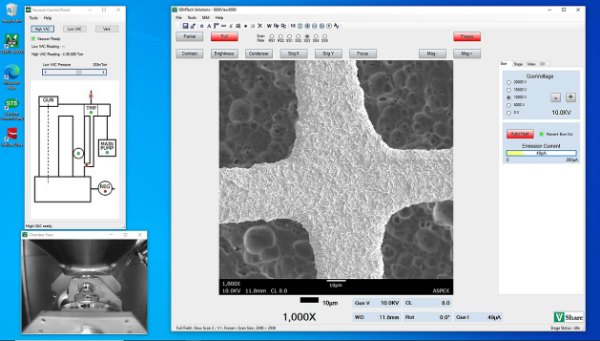
The FESEM has a vacuum issue and won’t be available for use until we can repair this. I have calls out to our service engineers and hope to know more soon.