Category: Electron Optics Facility News

Call for Content: ACMAL Micrograph

Micrograph showing a sample structure and 30 micron scale.

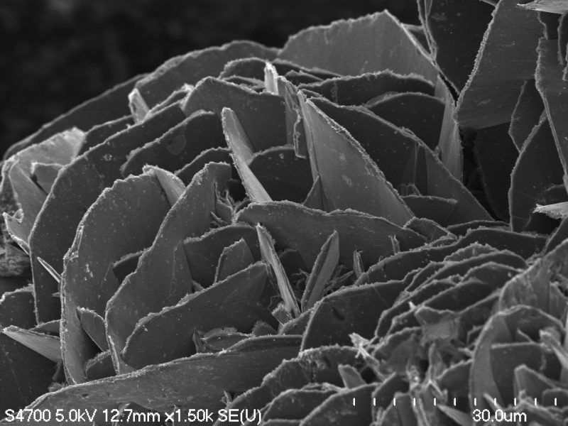
We at ACMAL are excited to announce that we are in the process of updating our micrograph posters.

We would greatly appreciate your valuable contributions to make them even more captivating. Though the initial focus is on electron images, we are also open to including other types of images, such as EDS/EBSD maps, that demonstrate the diverse range of analytical techniques available in our lab.

If you have captured any remarkable micrographs that you believe would be suitable for inclusion on our posters, we kindly invite you to share them with us. Your contributions will not only showcase your expertise but also contribute to the overall excellence of our collection.

To streamline the submission process, we have created an online form where you can easily upload your micrographs.

Micrograph Submission Form

We are eager to feature a diverse range of micrographs, highlighting the advancements and discoveries within the field of electron optics. Your submissions will help us showcase the remarkable work being done by our community.

Thank you in advance for your participation and for sharing your impressive micrographs. If you have any questions or require further assistance, please do not hesitate to reach out.

Upgrades for ACMAL’s Environmental Scanning Microscope

ESEM column and sample chamber.

The FEI Philips XL 40 Environmental Scanning Microscope (ESEM) is a large chamber scanning electron microscope. It is operated by a Michigan Tech shared facility, the Applied Chemical and Morphological Analysis Laboratory (ACMAL). ACMAL was awarded a Shared Facility Grant from the Associate Vice President of Research Development to upgrade the ESEM electronics and software system. The upgrade is expected to offset future repair costs and minimize instrument downtime.

If you have not considered the ESEM for your research, this instrument is capable of operating in high vacuum mode for conventional scanning electron microscopy.

The ESEM supports large area montage imaging and elemental mapping (up to a few square centimeters), energy dispersive spectrometer (EDS)-based phase analysis, chemical contrast imaging and EDS-based particle analysis, as well as crystallographic phase mapping, texture analysis and grain size orientation distribution by electron backscatter diffraction.

Contact ACMAL Director Elizabeth Miller with questions. You may request instrument training, sample preparation or sample analysis services. Remote training and collaboration are available. Request a tour for yourself and your team. We can help you select an instrument and find expertise in developing process plans for your research.

Current users are reminded to cite ACMAL in all publications arising from research using these instruments. Help us to build a community of electron microscopists.

Electron Crystallography in the TEM Seminar April 13, 2023

Erico Freitas operating the STEM.

Erico Freitas

Research Scientist, Materials Science and Engineering
Michigan Technological University

Electron Crystallography in the TEM: Using CBED to Determine Bravais Lattice, Point and Space Group, Lattice Parameters Refinement

Materials Science and Engineering Seminar

Thursday, April 13, 2023, 1 – 2 p.m.

Minerals and Materials Engineering Building (M&M) , 610

ACMAL Welcomes EOF Lab Assistants Zoe Hoffman and Maci Dostaler

We would like to officially welcome our two new lab assistants: Zoe Hoffman and Maci Dostaler. Also, congratulations to our previous senior lab assistant, Aleister Kerr. Aleister has taken a new position off campus and will no longer be working with us.

Zoe Hoffman

Zoe Hoffman is a current student at Michigan Tech majoring in Medical Laboratory Science with a minor in Pre-Health from southeast Michigan. She has always found the idea of working in a laboratory fun and likes to assist in the ACMAL‌ unit.

Maci Dostaler is currently an undergraduate student in Michigan Tech’s Biomedical Engineering program. She has lived in the Copper Country all of her life and is a proud first-generation college student. After graduation, she is hoping to work with imaging and non-invasive lasers. She is involved deeply around campus from volunteering to Greek life! In her free time she loves to challenge herself in snowboarding competitions both throughout the midwest and nationally.

You can contact Maci and Zoe if you need assistance with sample preparation or coating.

New Environmental Scanning Electron Microscope Proposal

Schematic of the microscope interior with specimen chamber, gun, pump, and gas valve marked.

Basic ESEM gas pressure stages, by Gerry Danilatos.

The Department of Defense (DoD) announces the Fiscal Year 2023 Defense University Research Instrumentation Program (DURIP). I’m excited to share that the 2023 DURIP selections have been announced and our proposal for a new Environmental Scanning Electron Microscope is recommended for award. All indications are that it will be funded. Congratulations to Dr. Bruce Lee (PI), Dr. Paul Sanders, Dr. Trisha Sain, Dr. Kazuya Tajiri, and Dr. Stephen Techtmann. Once funded, the new instrument will be housed in ACMAL and available for use by the MTU research community.

The timing is still TBD but since the project should be completed within a year we are starting the planning process to finalize the equipment purchase. However, there is still an opportunity to add capabilities to the instrument, especially if cost share can be contributed. Some possible additions include: a windowless EDS detector for light element (including Li) analysis, tensile stage, cryo stage, etc.

Below is a summary of the capabilities of the proposed new SEM.

Summary of the Capabilities and Functions of the Proposed FE-ESEM

Instrument

  • Environmental or Variable Pressure Scanning Electron Microscope

Electron Source

  • Field emission gun assembly with Schottky emitter source

Voltage

  • 20 V to 30,000 V

Resolution at 30 kV

  • High-vacuum Mode: 1.0 nm (SED) and 2.5 nm (BSED)
  • Low-vacuum Mode: 1.3 nm (SED) and 2.5 nm (BSED)
  • Environmental Mode: 1.3 nm (SED)

Magnification

  • 20x to 1,000,000x in a single quadrant

Ulti Max 170 EDS

  • Fast acquisition (quantitative > 400,000 cps and mapping > 1,000,000 cps)
  • Operate at low beam current, minimizing beam damage (3.5–5 kV)
  • High sensitivity for light element analysis

Symmetry S2 EBSD

  • High-speed analysis (indexing > 4,500 patterns per second)
  • High sensitivity >800 patterns per second/nA
  • Operates at low beam currents

Heating Stage

  • In-situ experimentation up to 1,100°C
  • Compatible with SE, BSED, EDS & EBSD detectors

Add Your Input

If you have any suggestions for capabilities or would like to discuss please contact Liz Miller by December 15th.

The Principal Investigator is Bruce Lee for research in additive manufacturing, materials development, and plastic waste recycling. The funding agency is the Office of Naval Research. DURIP is designed to improve the capabilities of accredited United States (U.S.) institutions of higher education to conduct research and to educate scientists and engineers in areas important to national defense, by providing funds for the acquisition of research equipment or instrumentation.

Erico Freitas Seminar September 29, 2022

Erico Freitas

Department of Biological Sciences Seminar Series

Dr. Erico Freitas

Research Scientist
Materials Science and Engineering
Michigan Technological University

Abstract

Dr. Freitas manages the FEI 200kV Titan Themis STEM in the Electron Optics Facility of the Applied Chemical and Morphological Analysis Laboratory (ACMAL) at Michigan Tech. Transmission electron microscopy (TEM) is widely used for morphological studies of biological systems as it offers a much higher spatial resolution (over 200 times) than optical microscopy. During this seminar Dr. Freitas will present the capabilities of the Scanning transmission electron microscope laboratory at MTU and will address the types of ex-situ and in-situ analysis that can be conducted for biological systems using a diversity of approaches available through the ACMAL.

For additional information, visit the Department of Biological Sciences.

Thursday, September 29, 2022
3–4 p.m. GLRC 202

ACMAL Welcomes Erico T. F. Freitas

Erico T. F. Freitas

Research Scientist Erico T. F. Freitas has joined ACMAL and Materials Science and Engineering. He will manage the FEI 200kV Titan Themis STEM in ACMAL’s Electron Optics Facility. Freitas has experience in nanostructured materials characterization, with specialties in TEM, STEM, EELS, EFTEM, EDX, and electron diffraction.

Freitas worked previously in the multiuser electron microscopy facility managing the TEM at the Universidade Federal de Minas Gerais, Brazil.