
Planting the Seeds of Research
Are you a:
- Tenured, tenure-track, or research faculty?
- Post-doctoral researcher?
- Michigan Tech staff member?
Are you planning to seek funds for research elsewhere, but require start-up money to develop your proposal?
If so, you are eligible to apply for Seedling Research Funding opportunities of up to $1,000.
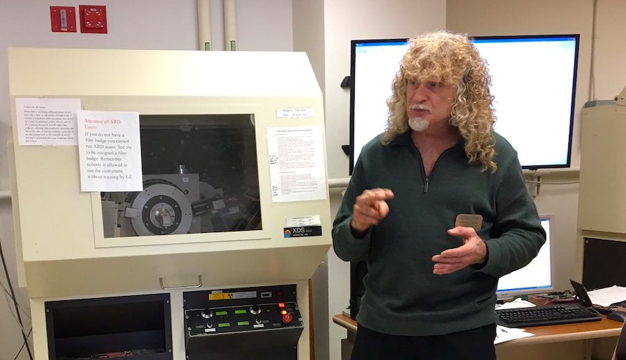
The Applied Chemical and Morphological Analysis Laboratory (ACMAL) at Michigan Tech has set aside $4,000 to fund pre-proposal research. These funds are designed to be granted to those who need to do preliminary investigations and data collection, which will then be used to develop a proposal for research funding from another source.


