Surface and Interface Science CH5665/MSE5665
(3 credits)
WF 1-2 p.m., M 1-3 p.m. (lab and analysis)
Learn To
- Understand the physical and chemical processes that influence surface chemistry and growth
- Apply surface science techniques to solve materials problems
- Proper data analysis and interpretation
- Design a project and solve a proposed hypothesis using surface analysis
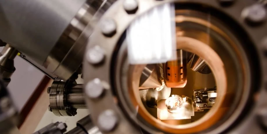
- Surface analysis methods: spectroscopy and microscopy techniques
- XPS, AES, surface sensitive-FTIR, HREELS, Raman, surface structure (LEED), TPD, AFM and ambient pressure techniques
- Applications in materials science, chemistry, physics, engineering, environmental science, catalysis, semiconductors and related tech industries

 Surface and Interface Science CH5665/MSE5665